A multigate device or multiple gate field-effect transistor (MuGFET) refers to a MOSFET (metal–oxide–semiconductor field-effect transistor) which incorporates more than one gate into a single device. The multiple gates may be controlled by a single gate electrode, wherein the multiple gate surfaces act electrically as a single gate, or by independent gate electrodes. A multigate device employing independent gate electrodes is sometimes called aMultiple Independent Gate Field Effect Transistor (MIGFET).
General MOSFET at submicron level is suffering from several submicron issues like short channel effects, threshold voltage variation etc. FinFET is proposed to overcome the short channel effects. Structure of FinFET is shown in Figure
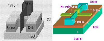
Silicon on insulator (SOI) process is used to fabricate FinFET. This process ensures the ultra thin specifications of device regions. In FinFET electrical potential throughout the channel is controlled by the gate voltage. This is possible due to the proximity of gate control electrode to the current conduction path between source and drain. These characteristics of the FinFET minimize the short channel effect. Advantages of the FinFET over its bulk-si counterpart are as follows:
Conventional MOSFET manufacturing processes can also be used to fabricate FinFET.
FinFET provides better area efficiency compared to MOSFET.
mobiblity of the carriers can be improved by using FinFET process in conjunction with the strained silicon process.
FinFET device structure Silicon on Insulator (SOI) process is used to manufacture FinFET. A single poly silicon layer is deposited over a fin. Thus poly silicon straddles the fin structure to form perfectly aligned gates. Here fin itself acts as a channel and it terminates on both sides of source and drain. In general MOSFET device, over the Si substrate poly silicon gate is formed. Poly silicon gate controls the channel. Straddling of poly silicon gate over the Si fin gives efficient gate controlled characteristics compared to MOSFET. Since gate straddles the fin the length of the channel is same as that of width of the fin. As there are two gates effectively around the fin we can write, width of the channel is equivalent to twice the height of the fin i.e. w=2*h. A term called “fin pitch” is used to define the space between two fins. Height of the FinFET is equivalent to width of the MOSFET. If w is the fin pitch then to attain same area efficiency required fin height is w/2. But practical experiments have shown that fin height can be greater than w/2 for a fin pitch of w. thus FinFET achieves more area efficiency than MOSFET.
The basic electrical layout and the mode of operation of a FinFET does not differ from a traditional field effect transistor. There is one source and one drain contact as well as a gate to control the current flow.
In contrast to planar MOSFETs the channel between source and drain is build as a three dimensional bar on top of the silicon substrate, called fin. The gate electrode is then wrapped around the channel, so that there can be formed several gate electrodes on each side which leads to reduced leakage effects and an enhanced drive current.
The manufacture of a bulk silicon-based multi gate transistor with three gates (tri gate) is described below.
Construction of a bulk silicon-based FinFET
1. Substrate: Basis for a FinFET is a lightly p-doped substrate with a hard mask on top (e.g. silicon nitride) as well as a patterned resist layer.
2. Fin etch: The fins are formed in a highly anisotropic etch process. Since there is no stop layer on a bulk wafer as it is in SOI, the etch process has to be time based. In a 22 nm process the width of the fins might be 10 to 15 nm, the height would ideally be twice that or more.
3. Oxide deposition: To isolate the fins from each other a oxide deposition with a high aspect ratio filling behavior is needed.
4. Planarization: The oxide is planarized by chemical mechanical polishing. The hard mask acts as a stop layer.
5. Recess etch: Another etch process is needed to recess the oxide film to form a lateral isolation of the fins.
6. Gate oxide: On top of the fins the gate oxide is deposited via thermal oxidation to isolate the channel from the gate elctrode. Since the fins are still connected underneath the oxide, a high-dose angled implant at the base of the fin creates a dopant junction and completes the isolation (not illstrated).
7. Deposition of the gate: Finally a highly n+-doped poly silicon layer is deposited on top of the fins, thus up to three gates are wrapped around the channel: one on each side of the fin, and - depending on the thickness of the gate oxide on top - a third gate above.
The influence of the top gate can also be inhibited by the deposition of a nitride layer on top of the channel.
Since there is an oxide layer on an SOI wafer, the channels are isolated from each other anyway. In addition the etch process of the fins is simplified as the process can be stopped on the oxide easily.
General MOSFET at submicron level is suffering from several submicron issues like short channel effects, threshold voltage variation etc. FinFET is proposed to overcome the short channel effects. Structure of FinFET is shown in Figure
Silicon on insulator (SOI) process is used to fabricate FinFET. This process ensures the ultra thin specifications of device regions. In FinFET electrical potential throughout the channel is controlled by the gate voltage. This is possible due to the proximity of gate control electrode to the current conduction path between source and drain. These characteristics of the FinFET minimize the short channel effect. Advantages of the FinFET over its bulk-si counterpart are as follows:
Conventional MOSFET manufacturing processes can also be used to fabricate FinFET.
FinFET provides better area efficiency compared to MOSFET.
mobiblity of the carriers can be improved by using FinFET process in conjunction with the strained silicon process.
FinFET device structure Silicon on Insulator (SOI) process is used to manufacture FinFET. A single poly silicon layer is deposited over a fin. Thus poly silicon straddles the fin structure to form perfectly aligned gates. Here fin itself acts as a channel and it terminates on both sides of source and drain. In general MOSFET device, over the Si substrate poly silicon gate is formed. Poly silicon gate controls the channel. Straddling of poly silicon gate over the Si fin gives efficient gate controlled characteristics compared to MOSFET. Since gate straddles the fin the length of the channel is same as that of width of the fin. As there are two gates effectively around the fin we can write, width of the channel is equivalent to twice the height of the fin i.e. w=2*h. A term called “fin pitch” is used to define the space between two fins. Height of the FinFET is equivalent to width of the MOSFET. If w is the fin pitch then to attain same area efficiency required fin height is w/2. But practical experiments have shown that fin height can be greater than w/2 for a fin pitch of w. thus FinFET achieves more area efficiency than MOSFET.
The basic electrical layout and the mode of operation of a FinFET does not differ from a traditional field effect transistor. There is one source and one drain contact as well as a gate to control the current flow.
In contrast to planar MOSFETs the channel between source and drain is build as a three dimensional bar on top of the silicon substrate, called fin. The gate electrode is then wrapped around the channel, so that there can be formed several gate electrodes on each side which leads to reduced leakage effects and an enhanced drive current.
The manufacture of a bulk silicon-based multi gate transistor with three gates (tri gate) is described below.
Construction of a bulk silicon-based FinFET
1. Substrate: Basis for a FinFET is a lightly p-doped substrate with a hard mask on top (e.g. silicon nitride) as well as a patterned resist layer.
2. Fin etch: The fins are formed in a highly anisotropic etch process. Since there is no stop layer on a bulk wafer as it is in SOI, the etch process has to be time based. In a 22 nm process the width of the fins might be 10 to 15 nm, the height would ideally be twice that or more.
3. Oxide deposition: To isolate the fins from each other a oxide deposition with a high aspect ratio filling behavior is needed.
4. Planarization: The oxide is planarized by chemical mechanical polishing. The hard mask acts as a stop layer.
5. Recess etch: Another etch process is needed to recess the oxide film to form a lateral isolation of the fins.
6. Gate oxide: On top of the fins the gate oxide is deposited via thermal oxidation to isolate the channel from the gate elctrode. Since the fins are still connected underneath the oxide, a high-dose angled implant at the base of the fin creates a dopant junction and completes the isolation (not illstrated).
7. Deposition of the gate: Finally a highly n+-doped poly silicon layer is deposited on top of the fins, thus up to three gates are wrapped around the channel: one on each side of the fin, and - depending on the thickness of the gate oxide on top - a third gate above.
The influence of the top gate can also be inhibited by the deposition of a nitride layer on top of the channel.
Since there is an oxide layer on an SOI wafer, the channels are isolated from each other anyway. In addition the etch process of the fins is simplified as the process can be stopped on the oxide easily.
This comment has been removed by the author.
ReplyDelete2018-2023 Global FinFET Technology Consumption Market Report@ https://www.grandresearchstore.com/semiconductor-and-electronics/global-finfet-technology-2018-2023-806
ReplyDelete